GaN Adoption Tag Archive

Six Reasons to Rethink Power Semiconductor Packaging

1927

Written by:

In my 40 years’ experience in power semiconductors I have visited thousands of customers, big and small, on every continent except Antarctica.

When the issue invariably turns to the packaging of the power semiconductor – transistor, diode, or integrated circuit – the requests for improvement fall into six categories:

  1. Can you make the package smaller?
  2. Can you reduce the package inductance?
  3. Can you make the product with lower conduction losses?
  4. Can you make the package more thermally efficient?
  5. Can you sell the product at a lower price?
  6. Can you make the package more reliable?

eGaN® FETs and integrated circuits from EPC have taken a very different approach to packaging power semiconductors – we have ditched the package altogether!

Pretty radical.

The reason for ditching the package in the first place was serendipitous.  As a fledgling startup, no company specializing in power semiconductor packaging wanted to be bothered with small volumes and high up-front engineering costs.  So we went with the idea of supplying our products in chipscale formats.

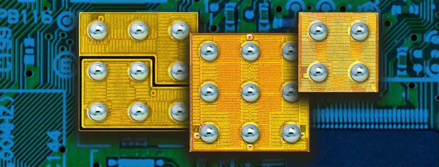
Figure 1 shows an EPC1001 transistor first introduced in March 2010.  This device has a thin layer of gallium nitride (GaN) grown on top of a standard silicon substrate.  Inside the GaN we fabricated a first-generation discrete transistor that performed 5 – 50 times better than the best silicon MOSFETs, depending upon the application.  And, instead of a plastic molded package, we put solderable bars directly on the surface of the device.  Flip this part over and it can be mounted it directly onto a PCB (See figure 2).


EPC1001

Figure 1:  The EPC1001 was first introduced in March 2010 and began the chipscale packaging revolution.


Pennypic

Figure 2:  Two EPC eGaN FETs are soldered to a PCB with the active area facing down.  The blue back surface is silicon nitride on top of silicon.


GaN-on-silicon has some amazing advantages over silicon power MOSFETs.  In addition to much, much superior device performance, the thin layer of GaN in which the active devices are manufactured can be sealed under multiple layers of glass during the standard fabrication process.  These layers of glass effectively protect the device from the environment, something silicon MOSFETs cannot do easily because the entire silicon-on-silicon structure is electrically active.  The lateral GaN devices are only active on the surface attached to the PCB.

When I was CEO of International Rectifier Corporation (now part of Infineon), we built about 1 billion MOSFETs every 6 weeks.  When all the expenses were added up, the cost of the packaging was equal to the cost of making the silicon chip inside the package.  The smaller the device, the higher the ratio of package-to-device cost.  Cutting out the packaging therefore cut out half the cost as well as a lot of the logistics required in the assembly process.  This significant cost reduction was a pretty good motivator to keep going with the chipscale packaging idea.

GaN transistors are much smaller than their silicon counterparts.  This size advantage translates into additional cost benefits to the GaN device maker, and it translates into additional cost benefits to the user.  PCB real estate is very expensive.  Smaller devices mean less real estate.  In some cases, the smaller footprint and greater performance of GaN enables a new end product not possible with larger silicon parts.  Figure 3 is my personal favorite example of the power of “small size.”  In this figure is a miniaturized X-ray machine in a pill that you swallow.  The result: the X-ray pill performs a colonoscopy without prior purging.  The high-resolution images of the colon are wirelessly transmitted to a receiver worn as a patch on the patient’s back. The cost of the pill is low enough that it does not have to be recovered after use (Whew!).  Can’t do it with silicon; just can’t.

Check Cap graphic

Figure 3: This X-ray pill from Check Cap can do a full colonoscopy without prior purging.  A high resolution image of the colon is beamed wirelessly to a receiver worn as a patch on the patient’s back.


Small has other advantages.  Small devices can be located closer to other devices in a circuit.  This reduces unwanted inductance.  Stray or parasitic Inductance is the enemy of a power system in that it causes the circuit to react more slowly and “ring” with voltage and current oscillations.  This ringing can damage devices in the circuit and cause unwanted noise that may need to be filtered out.

Figure 4 shows the impact of just the inductance inside silicon MOSFET packages on the power losses in a common power supply.  In this case, the internal package inductance causes the devices to turn on and off slower and therefore the transistor generates higher switching losses.  The popular SO-8 package induces losses that amount to 80% of the total losses incurred in the device.  Even the most efficient package – the DirectFET – doubles the losses in the device.  The EPC2001 chipscale device has less than 20% losses added due to inductance in the traces on the PCB under the device.  Lower losses, less heat, higher power conversion efficiency.  Oh, and the chipscale package also doesn’t add any unwanted resistance to the device.  Package resistance can add 20-50% to the resistance of a low voltage state-of-the-art silicon MOSFET.  Pure loss.

Chip-Scale Package eGaN FETs vs. Packaged MOSFETs

Figure 4:  Popular power packages such as the SO-8, LFPAK, and DirectFET add considerable parasitic inductance to a power conversion circuit.  This inductance induces large losses in the transistor inside the package.


Many customer, when they see the tiny eGaN transistors or ICs, worry about their ability to remove the heat from the part.  Power losses in the transistor generate heat. Thus, this heat must be removed or the device, and the entire system, may overheat.  The best way to get rid of heat is not to generate it in the first place.  In the above paragraphs we explained that GaN-on-silicon devices are much more efficient than silicon-based devices and therefore generate less power losses and less heat.

However, an amazing attribute of a package-less device is that it is much more thermally efficient than a MOSFET in the best power package.  Figure 5 is a comparison between eGaN FETs, double-sided QFNs, and DirectFETs.  In the figure, the vertical axis is the thermal resistance from the device to the ambient and the horizontal axis is the device size.  The lower the resistance the better, and eGaN FETs in chipscale “packages” are much better.  It is not a surprise, because eliminating all barriers between the active device and the ambient environment gives heat the most direct path to the outside world.

EPC Chip-Scale Packaged eGaN FET thermal Graph

Figure 5:  Chipscale packages have lower thermal resistance than the most efficient silicon packages.


Size, inductance, conduction losses, thermal resistance, and cost – chipscale beats packages every time!

What about reliability?

Experienced users and producers of power semiconductors will all tell you that it is the package that causes the most reliability problems.  Packaging induces high stress on the silicon device during the encapsulation processes.  Multiple dissimilar materials are used in a package to create a protected and sealed environment, but these dissimilar materials tend to grind against each other and come apart during thermo-mechanical stress.

Over 6 years and 17 billion device hours, eGaN FETs and ICs from EPC have demonstrated an unprecedented record of reliability in the field. Whether it be in truck headlamps, on board autonomous vehicles, inside 4G/LTE base stations, or within DC-DC power supplies, eGaN FETs have demonstrated a total field failure rate of under 1 FIT (Failures every billion device hours).  Figure 6 is a year-by-year record of eGaN FET field reliability.

EPC Chip-Scale Package eGaN FET Reliability

Figure 6:  Field reliability results for eGaN FETs.  As of January 2016, EPC has documented over 17 billion hours in the field.

The six key attributes of a better package, size, inductance, resistance, thermal efficiency, cost, and reliability all point to the future of packaging for GaN FETs and ICs as being – package-less — that is, no package at all!

Continue reading

Mid-Year Checkup on 2016 Predictions

1905

Written by:

Prognosticators do not often risk their reputations by giving their predictions a “checkup” midway through the period of their predictions. But, I am going to give it a shot and here we go…
Wireless Power Will Become Mainstream

Wireless power will continue to gain traction with increased consumer demand charged by new products and applications. There are two different standards vying for consumer adoption; Qi and AirFuel, but the consumer need not worry about a standards war because companies like Hewlett Packard are launching multi-mode systems that work on all standards. Consumers, in the meantime, will demand and buy these products in droves, further propelling development, as people put an end to their frustration with batteries and wires. In short, 2016 will be the year that wireless power “arrives.”

2016 predictions_1

Checkup: Computex, Taiwan’s cutting-edge technology trade show held last month, showed many new wireless charging products. Included in the announcements wereDell’s new notebook computer with AirFuel® charging capability, and also a charging pad for notebooks from WiTricity. In addition, LG Innotek showed a family of AirFuel compliant phones that will be hitting the market shortly, electric vehicle standards for charging devices in the car have been set, and multi-mode wireless transmitting systems are beginning to eliminate the confusion between Qi and AirFuel™ standard receiving devices. I think this prediction is coming true on schedule…and gaining speed!


Augmented Reality Stakes Its Place Alongside Virtual Reality

A seemingly unlimited amount of ink was spilled in 2015 discussing the promise of virtual reality. In 2016, however, there will be as much talk about augmented reality, as developers generate a slew of exciting applications across a variety of industries that add interactivity to the virtual world. Augmented reality will increasingly be used for such purposes as 3D product design, remote surgery, and education training (to name a few). While virtual reality is primarily confined to entertainment, the use cases for augmented reality are seemingly limitless. The affordability of augmented reality products will begin to become its own reality in 2017.

AR Glasses

Checkup: Pokemon Go has dominated the consumer product news cycle since its introduction earlier this month. Whereas it is a primitive form of the technology, it is demonstrating the appetite the consumer has for having access to an augmented reality.Magic Leap, a startup company working on a head-mounted virtual retinal display, which superimposes 3D computer-generated imagery over real world objects, is another example of the wave that is building for augmented reality applications. This pre-revenue startup has already raised more than $1.2B based on their uniquely realistic technologies. Hololens, Microsoft’s mixed reality head-mounted smartglasses, continue to move forward through the developers’ gauntlet bringing anticipation for the technology along with the journey. I think this prediction is coming true on schedule…if not ahead of schedule!


Autonomous Cars Will Advance – But Keep Both Hands on the Wheel for Now

While the technology to enable autonomous vehicles will advance, we are still a few years away from the proliferation of consumer driven autonomous vehicles, as we work out the technology and the regulatory issues. In future years, autonomous vehicles will enable much greater use of smartphones as drivers become passengers. Which, in turn, will drive demand for greater wireless bandwidth, 5G implementation, and wireless charging in our cars to prevent smartphones from running out of battery power. In the meantime, we will see more and more autonomy of vehicles under specific driving circumstances such as parking, freeway driving, and low speed stop-and-go.

2016 predictions_3

Checkup: Please keep your hands on the wheel! Recent incidents with Tesla autopilot have demonstrated that autonomous cars are still a long way from broad consumer readiness. However, more automated features such as auto-park, auto-braking and lane control are appearing in high-end vehicles. I think this prediction is coming true on schedule.


Internet Enablement In Underdeveloped Nations Will Grow at a Greater Clip

While most people on the planet are still without Internet access, coverage via wireless technologies will continue to accelerate.  Balloons (such as Google Loon), satellites (such as the Google-SpaceX venture), and high altitude drones (Facebook) are the most likely solutions to serve much of the underdeveloped world in the coming years and decades.

Google Loon

Checkup: AT&T recently announced they will start using drones at sporting events and concerts to enhance wireless cell phone coverage. That’s a great way to test and improve a technology in preparation for entering a potentially huge new and underserved market in developing countries.  Still moving forward on schedule with this forecast.


Improved Medical Diagnostics Will Gain More Attention

New, early detection techniques such as nano-RNA and micro imagining will make significant inroads towards early detection of certain types of cancers. For example, x-ray-in-a-pill colonoscopies will gain European approval in 2016 and will eliminate the key barriers to early detection of Colon Cancer. US approval is expected in 2017.

colonoscopy pill

Checkup: On schedule!


Moore’s Law Continues its Decline

Moore’s Law – the technology pact conceived by Intel co-founder Gordon Moore some 50 years ago – will continue its marked decline. Even Intel is backing away from this promise. As silicon fails to deliver on the advancement delivered in yesteryear the pace of technology progress will continue to stall, leading to reduced innovation and slowed end-market development. Technology companies will continue looking for alternative solutions to propel advancement to previous performance increase and cost reduction standards in order to fuel their new product pipelines and foster innovation.

Checkup: Intel is exploring new technologies including GaN as a possible successor to silicon in digital systems. In the meantime, EPC’s eGaN technology crossed the cost barrier with silicon in power conversion and continues to make inroads in the $30B market for power conversion semiconductors. Another correct prediction.

GaN Will Continue To Power Advancement

The ability to fuel technology advancement, including the applications above, will require significantly increased speed, voltage, bandwidth and efficiency, not to mention meaningful miniaturization. As silicon reaches its performance limitations, other new entrants are delivering significantly greater performance with rapidly decreasing costs and hundreds of new applications in mainstream markets. Independent GaN companies will set the pace while established power silicon producers will downplay the significance of the technology.

Checkup: It’s happening. GaN-on-silicon technology will displace silicon broadly in the $30B power conversion market due to a combination of higher performance, smaller size, AND lower cost. I am looking forward to seeing how my predictions finish the year and give thought to the emergence of applications using GaN technology can make in 2017!

Continue reading